PCB Manufacturing Service
PCB Manufacturing Process
1.Pre-Production Engineering
After we make a PCB order in NextPCB website, first engineers inspect our uploaded PCB file, it conducts a DFM review by checking the trace widths, the space between the traces, hole size etc and ensure the design is error free and fits within manufacturing capabilities. After checking several circuits, they combine them on a large production panel which is much more efficient to handle through the factory thus the production cost also decreases.
2.Board Cutting
In the table below is a key PCB capability list of NextPCB’s printed circuit board manufacturing. This table is designed to help you understand if our capabilities are a match for your design.It will also allow you to plan ahead and create your design within these capabilities so that you can be sure we can produce your PCB.
3.Drilling
After cutting the boards, they come to the drilling room. Drilling is done for two purposes. For connecting the leaded components and for the via holes that link the copper layers together. First the operator takes a MDF board as exit material, then he loads one or more PCB panels and place it on the machine, and finally adds a sheet of aluminum as entry foil. Those machines are computer-controlled, after selecting the right drill program the machine starts working, Drill change is fully automatic. The machine selects the drill to use from the drill rack and checks that it is the correct size, and then loads it into the drill head. This is a air driven drill which can rotate up to 150,000 revolutions per minute, the high speed drills makes the hole walls cleaner.
4.Deburr
After that the corners are trimmed to make it rounded, then the surface is cleaned and the machines automatically smooth the edges of the boards.
5.Electroless Copper Deposition
As the Board has drilled for making connection between top and bottom layer but the middle layer is nonconductive fiber glass, so to make connection between top and bottom layer the board comes for electroplating. The operator loads the panels onto the flight bars, the panels themselves act as cathodes for electroplating. The panels are carried through a series of chemical and rinsing baths by the overhead crane. This is a multi-stage process and everything is controlled by computer to ensure about 1-micron thick copper has deposited over the walls of the hole.
6.Copper Plate
Before the electroplating, the PCBs need to be micro-etched to roughen the surface of the boards , strengthen the bonding force of copper ions, and remove the residue and oxide on the boards surface to avoid contamination of the copper plating tank. After that the board goes through a series of process, where copper is plated up to a thickness, depending on the required final finish for the panel. This process took about 40 min of time, and then the board automatically goes to another room for next step.
7.Image Expose
To enter into this room, we need to put on a special type of Anti-Static Clothes, and we need to pass through a dust cleaning chamber. Then panel is first coated with a layer of photosensitive film, the photoresist, which is hot-rolled onto the copper. This machine does this automatically or sometime done this process manually. This film is blue light sensitive so all the lights into the room is yellow, so the light does not affect this film. Then the operator cleans the films, the film is the one which already has the printed circuit diagram on it and loaded the first film, then put the laminated panel and finally the second film. After perfectly aligning both layers, the board is sent to the Printer. The printer uses powerful UV lamps to harden photosensitive film according to the circuit printed film. So, after this process only the circuit part is hardened and rest unwanted areas remain soft. Modern machine can do this whole process automatically.
8.Image Develop
Next the board is processed through a chemical solution or developer that removes the unhardened and unwanted resist from areas that were not polymerized by light. After this you can clearly see only the circuit is printed by blue resist, and this material will resist the chemical at the etching process.
9.Inner Layer Etch
Then the board is sent for the etching, this process is to remove the unwanted copper using a powerful alkaline solution. After etching, the boards need be cleaned and washed to remove the excess chemical solution.
10.Automatic Optical Inspection (AOI)
Then the boards come for Automatic optical inspection or AOI, this machine enables fast and accurate inspection of PCBs to ensure that the quality of product leaving the production line is high and the items are built correctly and without manufacturing faults. When detecting the circuits, the machine automatically scans the PCB through the camera, collects images, and compares the tested solder joints with the qualified parameters in the database. After image processing, the defects on the PCB are checked and marked on the display screen for operators to repair.
11.Solder Mask Application
When everything is ok then the board comes again to another yellow room for solder mask. This coating machine simultaneously covers both sides of the panel with the epoxy solder mask ink. Solder mask is required to protect the copper surface and prevent solder shorting between components during assembly.
12.Bake
After applying solder mask, panels are now racked and put through a conveyorized drier at 87°C which hardens the resist just enough for the next stage. Usually it takes almost 25 minutes to bake.
13.Rescue Solder pad
Solder mask is applied to all over the board so to remove the solder mask from solder pad, first the operator takes the PCB and then align the photo film carefully at both side simultaneously. The UV lamps in the machine harden the ink where the film is clear. Later on, the unhardened and unwanted resists are stripped off.
14.Legend
Most PCBs have a component legend to show which component goes where, they use inkjet printers to image the legends direct from the board digital data. This printer is very advanced, the operator only needs to find the silk screen file corresponding to the board and set the positioning on the main control computer, then the ink will be applied on the boards evenly and automatically. Morevoer, it can also do printing and curing on the same system.
15.Surface finish
To protect the copper of Solder pad from oxidation hot-air solder leveling is often chosen as surface finish method for circuit boards. First the panels are being coated with flux, then the panels are dipped completely into a bath of molten solder, the solder covers all exposed metal surfaces. As the panel is removed from the solder, high pressure hot air blast removes excess solder from the holes and smooth the surface of the pads. In addition to the usual HASL, NextPCB also provides a variety of surface treatment methods, such as immersion gold, hard gold and OSP, for customers to choose according to their needs.
16.Electrical test
Finally, the PCB production process is done, then they electrically test every multilayer PCB against the original board data. Using flying probe tester they test the high voltage insulation and low resistance conduction of the circuit boards and check each net to ensure that the circuit is complete and there is no short or open circuit , for high volume production they use automatic e test machine which saves time and money because it runs at a high rate and eliminates the need for special fixtures.
17.Outline process -Rout, v-scoring, Bevel
After all testing, the boards come into the milling room, now it’s time to separate all individual PCBs from the large production panel, the operator loads one or more PCBs on to the CNC machine and choose the right program for those boards. According to customers need, the Board or arrays can also be V - scored so that they can easily be broken apart after assembly.
18.Wash boards
After milling the boards comes for cleaning, this machines cleans dust & oil stains which is generated during the shape processing and the production process, after wet cleaning the boards Are dried.
19.Final Inspection
Then a team of sharp-eyed inspectors give each PCB a final & careful check-over. She looks for any cosmetic defects like scratches & marking also checks aperture, thickness, holes etc. After inspection the PCBs are vacuum-sealed & bubble-wrapped to keep out dirt and moisture. Then the packets come to the packing room, after printing out the production release note, PCB’s are securely boxed inside foam wrapper and at the end of the day courier comes and took the packages, and NextPCB delivers them to all over the world.
| Items | Manufacturing Capabilities | Notes | Patterns |
|---|---|---|---|
| Layer count | 1 - 32 layers | Quantity of copper layers on the board | / |
| Impedance | For 4, 6, 8, 10, 12, 14, 16, 18, 20 layers PCB, PCB Stackup designed by NextPCB(by default), or PCB Stackup designed by customers | Layer Stackup Structure Impedance Calculation Parameter | / |
| Impedance tolerance | ±10% | / | / |
| Material | FR-4 | FR-4: TG130/TG150/TG170 | 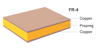 |
| PCB material dielectric constant | 4.2 | Prepreg dielectric constant (prepregtype: 7628/1080/2313/2116, dielectric constant: 4.2) | / |
| Max. dimension | 1-2 layers: 500*600mm 4-20 layers: 400*500mm | The maximum dimension that NextPCB can do | 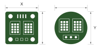 |
| Min. dimension | Length and width ≥10mm | Min. dimension = 10*10mm | / |
| Dimension tolerance | CNC: ±0.15mm, V-CUT: ±0.2mm | ±0.15mm for CNC routing, and ±0.2mm for V-scoring | / |
| PCB thickness | 0.6/0.8/1.0/1.2/1.6/2.0/2.5/3.0/3.2mm | The thickness of finished board | 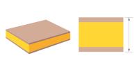 |
| Thickness tolerance ( Thickness≥1.0mm) | ±10% | e.g. If the board thickness is 1.6mm, the finished board thickness ranges from 1.44mm(1.6-1.6×10%) to 1.76mm(1.6+1.6×10%) | / |
| Thickness tolerance ( Thickness < 1.0mm) | ±0.1mm | e.g. If the board thickness is 0.8mm, the finished board thickness ranges from 0.7mm(0.8-0.1) to 0.9mm(0.8+0.1) | / |
| Finished copper weight | 1 oz/2 oz | Finished copper weight of outer layer could be 1 oz/2 oz | 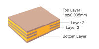 |
| Inner copper weight | 0.5 oz/1 oz/2 oz | Finished copper weight of inner layer could be 0.5 oz/1 oz/2 oz | 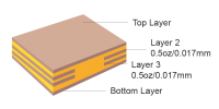 |
| Surface finish | HASL/Lead free HASL/ENIG/OSP | / | / |
| HDI structure | Rank 1 /Rank 2 /Rank 3 | Mechanical blind buried vias or laser blind buried vias(electroplating Via-filling is available) or laser blind vias filling dimple ≤ 15µm | / |
| Electrical test | Flying Probe/Special test fixture | No limits for Flying Probe. Max. 14000 Pads can be tested by PCB test fixture | / |
| Beveling angle of gold finger | 20°/30°/45°/60° | / | / |
| Beveling angle tolerance of gold finger | ±5° | / | / |
| Beveling depth tolerance of gold finger | ±0.1mm | / | / |
| Outline tolerance | ±0.15mm | / | / |
| V-CUT angle | 30°/45°/60° | / | / |
| Number of V-CUT | ≤30 cuts | / | / |
| V-CUT outline size | 55mm ≤ length/width ≤ 480mm | / | / |
| V-CUT residue thickness | 0.25mm ≤ v-cut residue thickness ≤ 0.4mm | / | / |
LATEST NEWS
CONTACT US
Whatsapp: (+86)18998453346
Phone: (+86)18998453346
Tel: (+86)18998453346
Email: [email protected]
Addr: TianHe District, GuangZhou, Guangdong Province, China
